The Rise of Advanced Semiconductor Packaging Technologies
1/15/2025 5:51:52 PM
As transistor miniaturization approaches physical limits, the semiconductor industry is undergoing a quiet revolution-shifting focus from shrinking chip geometries to reimagining how components are stacked, interconnected, and integrated. Advanced packaging technologies, including 2.5D/3D integration, fan-out wafer-level packaging (FOWLP), and heterogeneous integration, are emerging as critical enablers for next-generation electronics. This article explores how these innovations are driving performance breakthroughs in computing, IoT, and automotive systems, while reshaping the economics of chip design and manufacturing.
The Limits of Miniaturization: A New Frontier for Innovation
Moore's Law, which predicted doubling transistor counts every two years, has powered decades of exponential growth in computing power. However, with 3nm and 2nm nodes now requiring multi-billion-dollar investments and facing quantum tunneling challenges, scaling efficiency has plateaued. Transistor density gains have slowed to 15-20% per generation, down from 50% in the 2000s . This has forced the industry to look beyond 光刻 - based scaling, turning to packaging as a "second frontier" for performance enhancement.
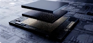
1. 3D Die Stacking: Vertical Integration for Density
3D integration involves stacking multiple dies (up to 12 layers in current designs) using through-silicon vias (TSVs) to create compact, high-bandwidth systems. TSMC's 3DFabric technology, for example, enables 12-layer logic-in-memory stacks with 10x faster data transfer than traditional 2D packaging . This is critical for AI accelerators, where data movement between processing units accounts for 90% of energy consumption. NVIDIA's H100 GPU uses 3D stacking to integrate 18,432 CUDA cores with 80GB of HBM2e memory, achieving 3x higher performance per watt than its 2D predecessor .
2. Heterogeneous Integration: Mixing and Matching Chips
Heterogeneous integration combines dies from different processes (e.g., 7nm logic, 22nm analog, or III-V compound semiconductors) in a single package, enabling tailored functionality without monolithic design compromises. Intel's Foveros 3D packaging allows integrating x86 cores, GPUs, and AI accelerators from different process nodes, delivering 50% higher performance per watt for laptop CPUs . This approach is also transforming automotive electronics, where heterogeneous packages consolidate power management, sensor processing, and high-speed connectivity into ruggedized modules capable of operating at 125°C .
3. Fan-Out Packaging: Shrinking Form Factors
Fan-out wafer-level packaging (e.g., TSMC InFO, Samsung eWLB) redistributes I/O pads around the die perimeter, eliminating the need for traditional organic substrates. This reduces package size by 40% compared to flip-chip BGA while enabling finer pitch interconnects (down to 30μm) . Apple's A-series chips have used InFO packaging since the iPhone X, achieving industry-leading power efficiency by integrating the APL CPU, M-series coprocessor, and NPU in a 9mm² package-smaller than a dime .
Impact on Industry Landscape and Applications
1. Redefining Design Economics
Advanced packaging lowers the barrier to entry for specialty chip developers. Startups like Graphcore and Cerebras can design large-scale AI processors using off-the-shelf 16nm dies, relying on 3D stacking to achieve performance comparable to leading-edge 5nm monolithic chips . This shifts value from pure foundry process nodes to packaging expertise, creating new opportunities for OSATs (outsourced semiconductor assembly and test) like Amkor and SPIL, which now account for 45% of global packaging revenue .
2. Enabling Next-Gen Applications
Edge Computing: Compact 3D packages allow integrating sensors, processors, and wireless radios in sub-10mm³ devices for industrial IoT, enabling real-time analytics in harsh environments.
Quantum Computing: Heterogeneous integration combines superconducting qubits with silicon control electronics, as seen in IBM's 127-qubit processor, which uses 2.5D packaging to minimize crosstalk between cryogenic components.
Healthcare Electronics: Implantable devices benefit from fan-out packaging's hermetic sealing and low power draw, enabling multi-year battery life for neural stimulators and glucose monitors.
3. Sustainability Synergy
By extending the lifespan of older process nodes (28nm and above account for 60% of global wafer starts ), advanced packaging reduces reliance on energy-intensive leading-edge fabs. A 2024 report by Yole Développement estimates that heterogeneous integration can cut chip development costs by 30% while reducing carbon footprint per transistor by 40% compared to monolithic designs .
Challenges and Future Directions
Despite its promise, advanced packaging faces technical hurdles: thermal management in dense 3D stacks (current solutions limit power density to ~150W/cm²), yield loss from multi-layer assembly, and lack of standardized design tools. The industry is responding with innovations like hybrid bonding (replacing solder bumps with copper-copper direct bonding for 10x higher interconnect density) and AI-driven package optimization, which can reduce design cycles from 18 months to 6 .
Looking ahead, the convergence of packaging and system design-dubbed "More than Moore"-is set to drive a decade of innovation. As the International Roadmap for Devices and Systems (IRDS) forecasts, advanced packaging will enable systems with 100x higher bandwidth, 50x lower latency, and 10x better energy efficiency by 2030 . For an industry once bound by lithography limits, the packaging revolution offers a path to continued progress-one layer at a time.
The Limits of Miniaturization: A New Frontier for Innovation
Moore's Law, which predicted doubling transistor counts every two years, has powered decades of exponential growth in computing power. However, with 3nm and 2nm nodes now requiring multi-billion-dollar investments and facing quantum tunneling challenges, scaling efficiency has plateaued. Transistor density gains have slowed to 15-20% per generation, down from 50% in the 2000s . This has forced the industry to look beyond 光刻 - based scaling, turning to packaging as a "second frontier" for performance enhancement.
Advanced packaging addresses two core challenges: functional integration (combining different chip types like logic, memory, and sensors) and performance optimization (reducing signal delay and power loss through shorter interconnects). By stacking dies vertically or arranging them in 2.5D configurations, companies can achieve equivalent performance gains to 2-3 generations of process node scaling-at a fraction of the cost .
1. 3D Die Stacking: Vertical Integration for Density
3D integration involves stacking multiple dies (up to 12 layers in current designs) using through-silicon vias (TSVs) to create compact, high-bandwidth systems. TSMC's 3DFabric technology, for example, enables 12-layer logic-in-memory stacks with 10x faster data transfer than traditional 2D packaging . This is critical for AI accelerators, where data movement between processing units accounts for 90% of energy consumption. NVIDIA's H100 GPU uses 3D stacking to integrate 18,432 CUDA cores with 80GB of HBM2e memory, achieving 3x higher performance per watt than its 2D predecessor .
2. Heterogeneous Integration: Mixing and Matching Chips
Heterogeneous integration combines dies from different processes (e.g., 7nm logic, 22nm analog, or III-V compound semiconductors) in a single package, enabling tailored functionality without monolithic design compromises. Intel's Foveros 3D packaging allows integrating x86 cores, GPUs, and AI accelerators from different process nodes, delivering 50% higher performance per watt for laptop CPUs . This approach is also transforming automotive electronics, where heterogeneous packages consolidate power management, sensor processing, and high-speed connectivity into ruggedized modules capable of operating at 125°C .
3. Fan-Out Packaging: Shrinking Form Factors
Fan-out wafer-level packaging (e.g., TSMC InFO, Samsung eWLB) redistributes I/O pads around the die perimeter, eliminating the need for traditional organic substrates. This reduces package size by 40% compared to flip-chip BGA while enabling finer pitch interconnects (down to 30μm) . Apple's A-series chips have used InFO packaging since the iPhone X, achieving industry-leading power efficiency by integrating the APL CPU, M-series coprocessor, and NPU in a 9mm² package-smaller than a dime .
Impact on Industry Landscape and Applications
1. Redefining Design Economics
Advanced packaging lowers the barrier to entry for specialty chip developers. Startups like Graphcore and Cerebras can design large-scale AI processors using off-the-shelf 16nm dies, relying on 3D stacking to achieve performance comparable to leading-edge 5nm monolithic chips . This shifts value from pure foundry process nodes to packaging expertise, creating new opportunities for OSATs (outsourced semiconductor assembly and test) like Amkor and SPIL, which now account for 45% of global packaging revenue .
2. Enabling Next-Gen Applications
Edge Computing: Compact 3D packages allow integrating sensors, processors, and wireless radios in sub-10mm³ devices for industrial IoT, enabling real-time analytics in harsh environments.
Quantum Computing: Heterogeneous integration combines superconducting qubits with silicon control electronics, as seen in IBM's 127-qubit processor, which uses 2.5D packaging to minimize crosstalk between cryogenic components.
Healthcare Electronics: Implantable devices benefit from fan-out packaging's hermetic sealing and low power draw, enabling multi-year battery life for neural stimulators and glucose monitors.
3. Sustainability Synergy
By extending the lifespan of older process nodes (28nm and above account for 60% of global wafer starts ), advanced packaging reduces reliance on energy-intensive leading-edge fabs. A 2024 report by Yole Développement estimates that heterogeneous integration can cut chip development costs by 30% while reducing carbon footprint per transistor by 40% compared to monolithic designs .
Challenges and Future Directions
Despite its promise, advanced packaging faces technical hurdles: thermal management in dense 3D stacks (current solutions limit power density to ~150W/cm²), yield loss from multi-layer assembly, and lack of standardized design tools. The industry is responding with innovations like hybrid bonding (replacing solder bumps with copper-copper direct bonding for 10x higher interconnect density) and AI-driven package optimization, which can reduce design cycles from 18 months to 6 .
Looking ahead, the convergence of packaging and system design-dubbed "More than Moore"-is set to drive a decade of innovation. As the International Roadmap for Devices and Systems (IRDS) forecasts, advanced packaging will enable systems with 100x higher bandwidth, 50x lower latency, and 10x better energy efficiency by 2030 . For an industry once bound by lithography limits, the packaging revolution offers a path to continued progress-one layer at a time.
Related information


- Help you to save your cost and time.

- Reliable package for your goods.

- Fast reliable delivery to save time.

- Quality premium after-sale service.